
ASML (Deep Dive)
''Never sell ASML'' - Full investment Thesis

1. Introduction

ASML is arguably the most important company in the world right now, a keystone player in the AI infrastructure revolution and in nearly all tech-related advancements. They are well known for their large moat, but in my opinion, ASML is still underappreciated by the masses.
It’s a company that’s hard to fully grasp and truly wrap your head around. In this deep dive, I will do my best to explain what ASML does and whether I think it’s a good investment or not.
Since I’m Dutch myself, I might be slightly biased. We Dutch people are quite proud of ASML. In the southern part of the Netherlands, I don’t think there’s a single person who doesn’t know someone working there. I think it’s truly special that such a big and important company resides in the Netherlands.
But don’t worry, I’m going to be as objective as I can.
Let’s dive in!
2. Origin Story
“ASML, the company that we are all proud of in the Netherlands.”
ASML was founded in 1984 as a joint venture between Philips and ASM International, with the goal of developing advanced photo-lithography systems for semiconductor manufacturing, that was dominated by Japanese firms back then. The new company, which was originally called ASM Lithography, was tasked with developing advanced lithography systems.
In 1998, ASML launched its first production tool and soon became completely independent from Philips. ASML was first publicly listed in 1996 on the NASDAQ and Euronext Amsterdam. This provided them with the much-needed capital to accelerate R&D and expand globally.
The 2000s were the period when things really started going. They introduced the TWINSCAN dual-stage system, which boosted productivity, and pioneered immersion technology, allowing chips to be made with even smaller features by shining light through water.
Then came the next big leap: Extreme Ultraviolet (EUV) lithography. Starting in the 2010s, ASML pushed the boundaries of physics, developing systems that use light of a shorter wavelength to create the smallest, fastest, and most powerful chips to date.
This required acquiring key partners like Cymer (light sources) and Hermes Microvision (metrology), forming a what ASML calls a “Holistic Lithography” strategy. More on that later.
By the 2020s, EUV moved into high-volume manufacturing, with ASML shipping its 100th system and later unveiling the High NA EUV (EXE) platform.
ASML’s differentiated strategy, deep co-development with leading chipmakers like Intel, TSMC, and Samsung allowed it to outpace competitors technologically and fundamentally.
Their decisive long-term bet on extreme ultraviolet (EUV) lithography cemented its position as the sole supplier of next-generation lithography systems, and it transformed ASML from a ‘‘small’’ Dutch startup into a monopoly-like enabler of global semiconductor innovation.
3. Company Overview
3.1 Geography
ASML produces lithography machines for the semiconductor industry. I will explain the concept of lithography and the role that ASML plays in the overall sector more in-depth later in this deep dive. For now, all you need to know, without ASML there won’t be any technological advancements.
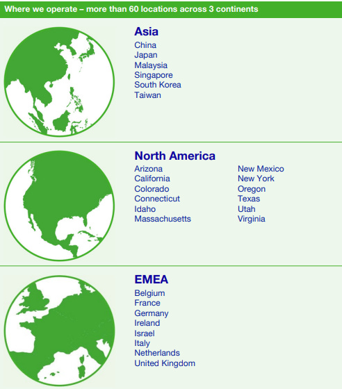
ASML is headquartered in the Netherlands and they currently employ about 44,000 people. ASML’s headquarter is in Veldhoven. Veldhoven is a relatively small place close to Eindhoven, which is known to be one of the bigger tech-hubs in the Netherlands. ASML
ASML’s campus in Veldhoven is like a small village. It’s huge. It has R&D and manufacturing hubs, massive cleanrooms and large office spaces. There’s a large central plaza where employees can eat, work and dine.

In addition to their Veldhoven headquarter, ASML has different sites around the world, primarily in the United States, Germany, and Taiwan. At these sites they conduct their R&D, manufacturing, and they also have some refurbishing activities.
3.2 Corporate structure
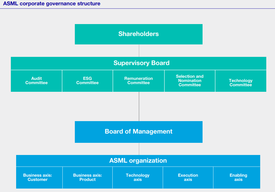
ASML’s corporate structure is quite straightforward. They have a two-tier board structure consisting of a Board of Management responsible for managing the company, and an independent Supervisory Board which supervises and advises the Board of Management. For the fulfillment of their duties, the two Boards are accountable to the General Meeting, the corporate body representing all shareholders.
4. Management
4.1 General
ASML’s management is known to be very long-term and strategically focused. One could argue they are quite conservative in their approach and communication. Their two latest earnings call really illustrate that. They use very conservative wording, and are very dismissive of making concrete guidance projections.
ASML’s core business is still cyclical. But, even though that’s the case, management does not seem concerned about short-term results but always focusses on the bigger picture. Guidance is given years ahead (2030) and short-term guidance is not sugarcoated and sometimes even non-existent.
If they are unsure, they are not afraid to take a more conservative stance. While investors may not always like that, as was the case after their Q2-earnings report, I quite like the fact that WHEN they give guidance, you can trust it.
While some companies have fancy and shiny CEO’s and board members, that is not the case with ASML. Most of the higher-ups have a technological background and to me, they seem quite down-to-earth and result-oriented.
So, who are the top guys (no women in upper management yet) for ASML?
4.2 CEO - Christophe Fouquet
In 2024 Christophe Fouquet replaced Peter Wennink. Who led the company from 2013 and 2024 and achieved spectacular results with ASML. The stock price went up over 1000% under his vision and leadership. Very tough shoes to fill, but so far Christophe is doing an excellent job.
Christophe Fouquet became President and CEO in 2024, having served as Executive Vice President EUV from 2018 until 2022, Executive Vice President and Chief Business Officer from 2022 until 2024 and member of the Board of Management since 2018. Since joining ASML in 2008, he has held several positions, including Senior Director Marketing, Vice President Product Management, and Executive Vice President Applications, a position he held from 2013 until 2018. Prior to joining ASML, he worked for semiconductor equipment peers KLA-Tencor and Applied Materials. Christophe holds a master’s degree in Physics from the Institut Polytechnique de Grenoble.
He is known for having a strong customer-centered approach and a focus on technological innovation. He believes collaboration is the key to success, which perfectly aligns with ASML extensive network of partners and key suppliers.

4.3 CFO - Roger Dassen
Roger Dassen is the Executive Vice President and Chief Financial Officer (CFO) and a member of the Board of Management at ASML, having joined the company in 2018. Before his tenure at ASML, he held high-level positions at Deloitte, where he was the Global Vice Chair and a member of the Executive Board, and previously the CEO of Deloitte Holding BV.
Dassen is highly educated, holding a Master’s degree, a post-master’s in Auditing, and a PhD in Business Administration from Maastricht University. Beyond his executive role, he is active in academia and public service, serving as a Professor of Auditing at Vrije Universiteit Amsterdam and holding board positions, including on the Supervisory Board of the Dutch National Bank and as Chair of the Supervisory Board for the Maastricht University Medical Center+.

4.4 CSS - Wayne Allan (Chief Strategic Sourcing)
Wayne Allan is the Executive Vice President and Chief Strategic Sourcing & Procurement Officer and a member of the Board of Management at ASML, a role he took on in 2023.
He has a long and deep history in the semiconductor industry, starting his career at Micron in 1987 as a production operator. He moved up the ranks through various roles in engineering, planning, and production before eventually serving as Senior Vice President of Global Manufacturing Operations and Vice President of Wafer Fabs at Micron. Allan joined ASML in 2018 as the Executive Vice President of Customer Support before transitioning to his current sourcing role. He is primarily responsible for managing ASML’s supply chain and supplier relationships at a strategic level

4.5 CCO - James Koonmen (Chief Customer Officer)
Jim Koonmen is the Chief Customer Officer (CCO) at ASML. He was appointed to the Board of Management in 2024. He has been with ASML for a long time, beginning in 2007 when he joined through the acquisition of Brion, where he served as General Manager. On his way up he held many leadership roles as the CEO of Cymer (an ASML unit) and then five years as the head of the Applications business line.
Before joining ASML, Koonmen gained diverse experience in technology and operations, including roles at MEMX, Onetta, and Johnson & Johnson. He is highly educated, holding two Master of Science degrees from the Massachusetts Institute of Technology (MIT), one in Aeronautics and Astronautics and the other in Management from the Sloan School.

4.6 COO - Frédéric Schneider-Maunoury
Frédéric Schneider-Maunoury is the Executive Vice President and Chief Operations Officer (COO) at ASML, a position he has held since joining the company in 2009 (and was appointed to the Board of Management in 2010).
His role is focused on managing the entire scope of ASML’s operations. Before ASML, he held leadership and manufacturing roles at the power and transportation group Alstom, where he served as Vice President of Thermal Products Manufacturing and General Manager of the worldwide Hydro Business. Early in his career he worked in the public sector, holding various positions at the French Ministry of Trade and Industry. He is a highly educated engineer, graduating from the prestigious École Polytechnique and the École Nationale Supérieure des Mines in Paris.

4.7 CTO Marco Pieters
ASML recently announced the appointment of Marco Pieters as Executive Vice President and Chief Technology Officer. Pieters has been with ASML over 25 years. He will focus on ASML‘s technology roadmap with a strong focus on customers needs.

4.8 Management Execution + summary
In the last few years, ASML’s management has been quite conservative in their approach. And management’s word reflect that conservative stance.
Two quotes that perfectly illustrate management conservative stance are the following:
Q2 earnings report:
ASML cannot confirm growth in 2026
Q3 earnings report
ASML does not expect 2026 total net sales to be below 2025
There are many ways to phrase these guidances, but they seem to always take the most conservative way of communicating. Is it a sign of weakness or just conservative? I think the latter.
Overall, I like ASML’s management. They seem level-headed, focused and long-term oriented. That perfectly fits my investing approach.
5. Semiconductor market
Companies in the semiconductor market basically produce and sell ‘‘chips’’, which are integrated circuits made from silicon, that power computers, phones, cars, industrial machines and even AI systems. It starts with chip design and ends with manufacturing and packaging in fabs.
I expect ASML to continue playing a key role in this semiconductor market for at least the next decade and very likely way longer. Since they virtually have no competitors, and are a so-called monopoly, they are and will be the only player that can manufacture the machines for the most advanced microchips.
Without ASML’s machines, chipmakers like TSMC, Samsung, and Intel cannot produce their products, effectively making ASML the key bottleneck in the upcoming AI and datacenter transition and anything else that we need the chips for.
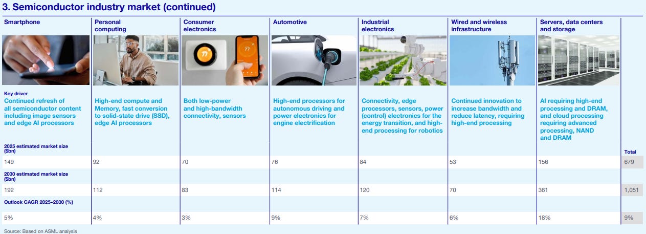
5.1 The TAM
So, how big is this overall semiconductor market actually?
Deloitte estimates that the semiconductor market will grow to $1T revenue by 2030. This is almost a double compared to 2024, in which the total came in just above $600B.
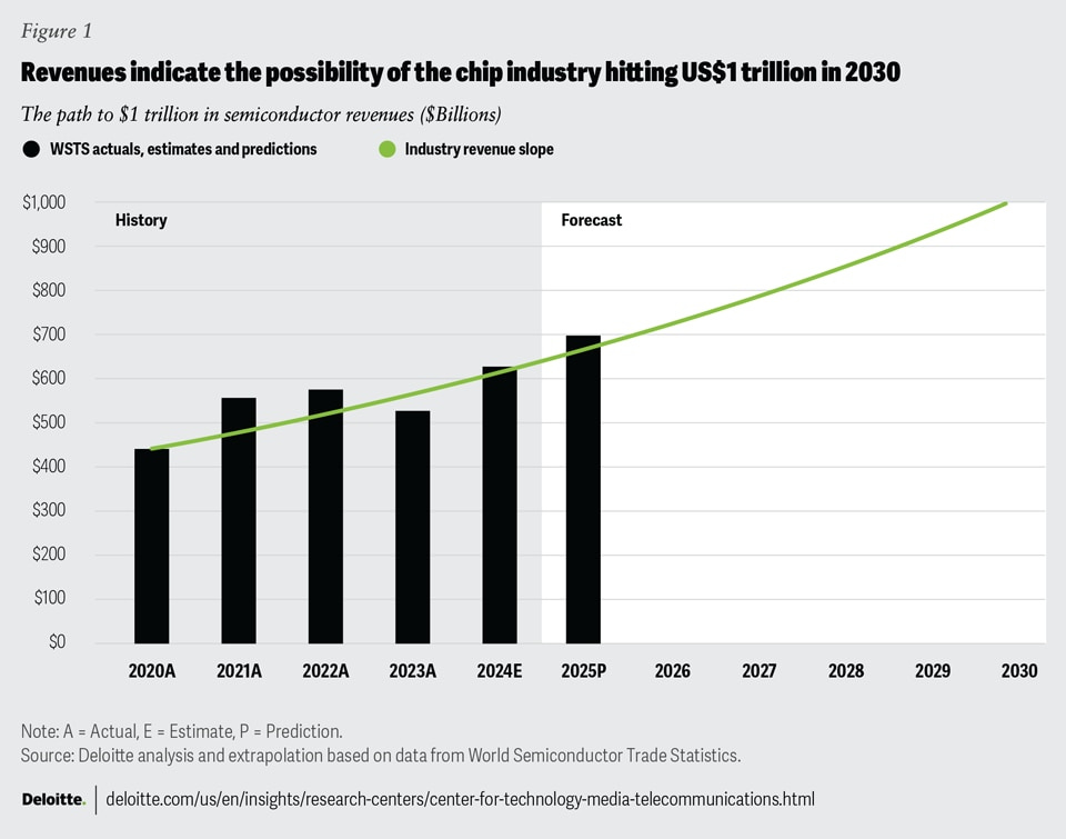
This growth trajectory is confirmed by PWC, as they came to the same conclusion. They also expect ‘‘the chip market’’ to reach $1T by 2030. This implicates a 7.7% CAGR from 2024 onwards. I expect ASML to exceed the 7.7% CAGR, but more on that later
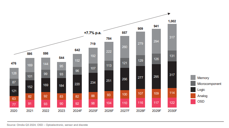
Of course, this is the overall semiconductor market. ASML covers a smaller part of that. The semiconductor market is mostly shaped by two main segments: logic and memory. These two groups generate the largest share of the overall market’s sales, and that trend is expected to continue towards 2030.
Their dominance comes from the core function they perform across nearly all modern technology. Whether its the high-end computing, mobile devices, or specialized industrial and automotive systems, these specific components are absolutely essential.
The accelerating global demand for processing and storing data, driven by the massive infrastructure build-outs in cloud computing and the proliferation of AI applications and the Internet of Things (IoT) will most likely ensure a substantial need for increasingly faster and more efficient logic and memory solutions, and therefore ASML’s chips.
ASML believes they can capture between €44B and €60B in sales by 2030. (this equates to $51.20B and $69.81B, based on the current EUR/USD (as of 08-10-2025).
Simply put, ASML is part of a long-term growth trend in the semiconductor market. With all the AI developments, I think this growth might even accelerate towards 2030.
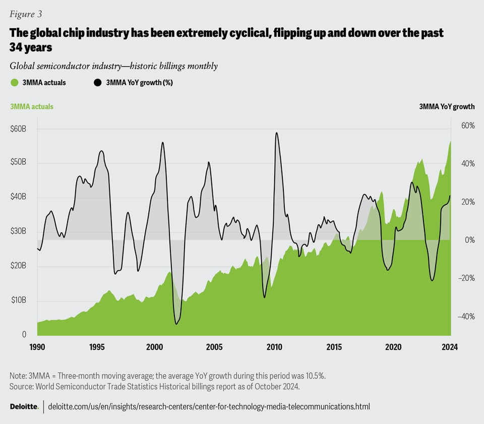
5.2 Cyclicality
One of the things some investors do not like about ASML and the semiconductor market, is the cyclical nature. One could argue this cyclical nature is even more prevalent in ASML itself, as they deal with the cyclicality of the overall market, but also the cyclicality and irregular lumpy revenue in their order books.
Net bookings don’t come in ‘‘gradually’’. since their machines are so expensive, and only a handful of big players can buy them, the orders come in fragmented throughout the business cycles.
Personally, I’m not worried about this, as this is just inherent to ASML’s business, but it can provide for some short-term headwinds and volatility. Below picture perfectly illustrates the cyclicality of the global chip market.
5.3 Semiconductor market ecosystem
The semiconductor market is a difficult intertwined system. Companies cannot exist without each other. The below picture is a nice representation of the ecosystem ASML operates in. If I had to change anything, I’d put ASML in the middle. Without ASML’s machines, this ecosystem simply cannot exist.
A great example of how this works is the chain that follows after Nvidia. Nvidia designs the chips for its GPUs and AI products, but it relies on TSMC to manufacture them, making TSMC its exclusive fabrication partner. Take one hard guess where TSMC gets the machines to manufacture NVDA’s chips from. Yes, you guessed it right.

5.4 Summary
ASML is set up well to benefit from long-term tailwinds in the overall semiconductor market. Their cyclical nature can be seen as a negative point, but for anyone with a long-term mindset, this should not worry you. As demand for chips increases, so will the demand for the machines that ASML makes.
ASML is perfectly set up to be a key backbone player in the AI revolution, the data-center buildout rush we see, but also just the sheer technological advancements that await in the next decade. We WILL need ASML, to produce these machines to make it all happen.
I will go into ASML’s customers and other key players in the semiconductor market later in this deep dive.
6. ASML’s Machines
ASML makes most of it’s money through the sales of their machines. But there are a few other parts of their business that also contribute significantly, and could turn out to be a bigger and more important part their business in the future.
First we dive into what lithography is, and then we analyse the different machines and segments. I will try to not get too technical, so it’s easy enough to understand without a technical background.
6.1 Lithography
To understand why ASML’s machines are so important, we first have to understand the bigger context. The machines that ASML produces, are so-called ‘‘lithography’’ machines. I’ll explain in short what that means:
Lithography machines are precision devices that project patterns onto silicon wafers to create tiny circuits which are found in modern electronics.
Using light sources, masks with circuit designs, and complex optical systems, these machines “print” these patterns, which are then chemically developed onto a photosensitive material (photoresist) on the wafer. This process is repeated to build up complex 3D chip designs.
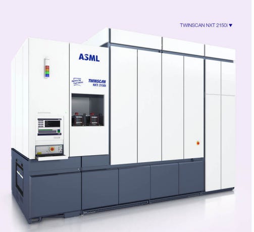
For reference, ASML’s machines cost about €300M on average, and their newest machines (high-na) cost up to €400M.
ASML’s machines have over 700,000 components. This total includes everything from the large structures to the individual parts required for chip lithography. To put this into perspective, a typical car has around 30,000 parts. This is not some ordinary machine.
It takes three Boeing 747 cargo planes to transport one current-generation EUV machine from ASML. Each machine is a logistical challenge, as its components are shipped in 40 freight containers, three cargo planes, and 20 trucks.
The video below explains perfectly how ASML’s machines work:
6.2 Moore’s law
So, ASML’s machines are used to produce chips. But how small are these chips? Well, there’s an ongoing search to make these chips ever more smaller and increase it’s computing power at the same time.
This is what we call: Moore’s law.
Moore’s Law is the observation and prediction that the number of transistors on an integrated circuit doubles approximately every two years, leading to exponential growth in computing power and a decrease in cost per transistor.
Gordon Moore, the co-founder of Intel, invented Moore’s Law in 1965, originally observing that the number of transistors on a microchip would double every year. He later revised this prediction to a doubling approximately every two years.
This isn’t a law of physics, but an empirical trend that became a guiding principle and motivation for the overall semiconductor industry.
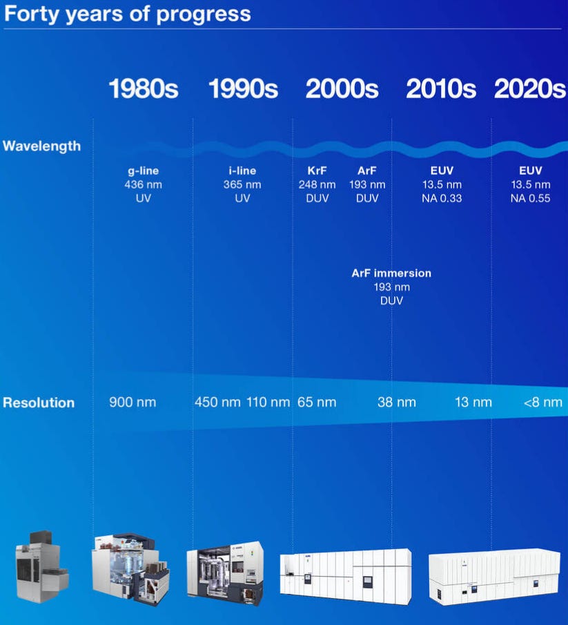
Below is an old slide, but it does paint a good picture of ASML’s roadmap during this chase of more compute and cost reduction:

Another, more recent picture shows the progress of the product range of ASML since 1980. We will cover the DUV and EUV machines next. ASML machines are capable of etching patterns as small as 8 nanometers, 1/10000 the width of a human hair
The two main segments for ASML’s business are DUV and EUV. We will cover these two first. Later we touch some different, lesser known segments which also contribute to ASML’s overall growth potential.
6.3 DUV
6.3.1 The systems
DUV (Deep Ultraviolet): These systems use DUV light (think 193 nm wavelength) and are widely used to mass-produce all kinds of logic and memory chips.
DUV lithography systems are the workhorses of the industry, producing the majority of layers in microchips. ASML offers both immersion as well as dry lithography systems, which use range of light sources to offer all wavelengths currently used in the semiconductor industry: argon fluoride (ArF) lasers for 193 nm wavelength, krypton fluoride (KrF) lasers for 248 nm and mercury vapor discharge lamps (i-line) for 365 nm.
These systems lead the industry in productivity, imaging and overlay performance and help manufacture a broad range of semiconductor nodes and technologies, and support the industry’s cost- and energy-efficient scaling.
6.3.2 Immersion and dry lithography
The distinction between immersion and dry DUV lithography lies in how light travels from the projection lens to the wafer, what may seem like a small difference actually has a major impact on resolution and chip scaling.
Dry DUV lithography is the ‘‘traditional’’ approach. In this method, there’s air between the lens and the wafer surface. The numerical aperture (NA), which determines how finely details can be printed, is limited by the refractive index of air (essentially 1.0). While this setup is simpler and highly effective for many mature semiconductor nodes, it eventually reaches physical limits in how small features can be printed.
Then we have Immersion DUV lithography, which introduces a thin layer of highly purified water between the final lens element and the wafer. Water has a refractive index of about 1.44, which allows the system to focus light more tightly, increasing the numerical aperture beyond what’s possible in air. This innovation effectively boosts resolution and enables smaller feature sizes without requiring shorter wavelengths.
Dry systems excel in cost-efficient production for established nodes and high-volume applications like sensors, analog chips, and power devices.
Immersion systems are used for advanced logic and memory manufacturing, where every nanometer of precision matters.
In essence, immersion lithography represents an evolution of the DUV platform, extending its usefulness deep into the nanometer era and bridging the gap between traditional optical lithography and today’s EUV technologies.
6.4 EUV
6.4.1 The system
EUV (Extreme Ultraviolet): This is ASML’s crown jewel. EUV machines use much shorter wavelength light (13.5 nm) to print the tiniest, most complex features on today’s most advanced chips. This shorter wavelength allows the machine to print features so small they are measured in a few nanometers, enabling modern processors found in smartphones and AI hardware.
Using EUV light at a wavelength of 13.5 nm, EUV lithography systems make it possible to print the smallest features on microchips at the highest density. They are used for the most intricate, critical layers on the most advanced microchips.
Since EUV light is absorbed by nearly everything, including air and glass, the machine operates in a near-perfect vacuum and uses a complex system of the flattest mirrors ever made, instead of lenses. The light is generated by blasting microscopic droplets of molten tin with a powerful laser fifty thousand times per second!
These EUV machines also help simplify ASML’s customers’ manufacturing processes, compared to complex multiple patterning strategies using deep ultraviolet (DUV) immersion systems. ASML is currently the world’s only manufacturer of these EUV lithography systems
ASML’s EUV machines aren’t allowed to be exported to China. DUV machines face some restrictions too, but they can still be sold there (for now).

6.4.2 HIGH-NA EUV
ASML is now rolling out High-NA EUV machines. High-NA EUV is the successor to the current EUV technology. Its purpose is to continue the industry’s ability to shrink chip features, enabling the move to 2nm process nodes and beyond. High-NA EUV machines are the most advanced generation of lithography tools out there right now.
The “High-NA” refers to the increase in the numerical aperture (NA) of the optical system, from 0.33 in current EUV to 0.55. This increase in NA is what gives the machine its higher resolution, allowing it to print patterns with a resolution of just 8 nanometers
To prepare High NA EUV (0.55 NA) for high-volume manufacturing, the first operational prototype was made available to chipmakers in the new ASML-imec High NA EUV Lithography Lab in Veldhoven campus. Two more TWINSCAN EXE:5000 systems were assembled and installed at an Intel plant near Hillsboro, Oregon and a fourth system was shipped to a customer in Asia.
In April 2024, the High NA EUV system in Veldhoven printed the first-ever 10 nm dense lines, with imaging done after optics, sensors and stages completed coarse calibration (see image on the right).
This important milestone showed the system is functioning, though not at full performance in a high-volume manufacturing environment yet

6.5 Metrology and inspections
Another part of ASML’s business, that is not so often talked about are their metrology and inspections systems. These systems enable chipmakers to measure printed wafers, which ensures they align with the intended designs. This supports chipmakers in optimizing patterning throughout every stage stage of the manufacturing process.
Inspection systems act as the fab’s early warning network. They scan wafers and masks for particles, pattern defects, and anomalies, classifying which ones threaten yield and which are benign. Optical inspection offers speed and coverage, while e-beam review tools confirm and characterize what truly matters.
These systems play a key role in ASML’s ‘‘holistic’’ approach, which we will discuss later. This segment can be divided in two parts:
6.5.1 Optical metrology
Optical metrology is the frontline tool for process control. Using light to measure overlay, film thickness, and critical dimensions, it delivers fast, non-destructive data across thousands of wafer sites. These readings feed directly into ASML scanners’ control loops, adjusting focus, alignment, and exposure in real time to keep each layer perfectly registered.
6.5.2 E-beam metrology and inspection
Where optical methods reach their resolution limits, e-beam metrology steps in. By scanning with a finely focused electron beam, it reveals nanometer-level details line edge roughness, critical dimension variation, and feature profiles. Though slower, it provides the “ground truth” needed to calibrate optical models and diagnose root causes when processes drift.
Together, these systems create a sort of defense against error: fast optical control, high-resolution e-beam verification, and defect inspection. Without them, even the most advanced lithography tools couldn’t maintain the precision required to operate perfectly.
6.6 Software and maintenance
On top of building and installing these machines, another big part of ASML’s business is software and maintenance.
They develop advanced software that works with their hardware. This is important, because ASML isn’t just there to drop off a machine, they are THE key partner for their customers throughout this entire process.
Because these machines are incredibly complex and expensive, ASML offers full-on customer support: installation, maintenance, upgrades, and even training for chipmakers all over the world. Customers rely on them from start to finish.
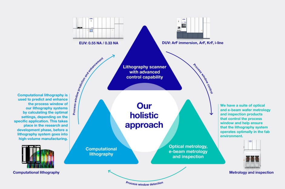
6.7 Holistic approach
ASML prides itself in it holistic approach. So what does that mean?
ASML’s holistic approach to lithography: integrates advanced hardware, computational lithography, metrology, and inspection into a unified ecosystem that enables chipmakers to develop, optimize, and control every aspect of semiconductor production.
At the core of this approach is the process window, which is basically the range of acceptable process variations within which chips can be reliably produced to specification. By combining so called computational models, real-time metrology, and intelligent inspection, ASML empowers customers to maximize this process window, ensuring system stability and high yield in high-volume manufacturing environments.
The result is a synergistic fusion of high-precision hardware and advanced software, designed to sustain Moore’s Law scaling and deliver more functional chips per wafer, per day. This integration strengthens ASML’s competitive moat and sets them up to be a backbone player in next-generation semiconductor manufacturing.
6.8 Summary
ASML builds the world’s most advanced lithography machines, the systems that “print” microscopic circuits onto silicon wafers, forming the foundation of every modern chip. Their technologies drive Moore’s Law, enabling chips to become smaller, faster, and more efficient every year.
The company’s DUV systems handle most chip layers, while the EUV and High-NA EUV machines define the new, more cutting edge part of semiconductor manufacturing.
Alongside these, ASML’s metrology, inspection, software, and services ensure every chip layer aligns with perfect precision.
Together, this integrated ecosystem, hardware, software, and process control, makes ASML the backbone of the global semiconductor industry.